
The U.S. government is footing the bill, yet MojoVision still has to pay a “physical tax”: the technological cost of switching from blue-light Epitaxy to full-color technology.
Introduction
On October 20 (Eastern Time), U.S.-based Micro LED platform company MojoVision announced it has secured $24.4 million (approximately RMB 163 million) in U.S. government funding to develop a monolithic, full-color Micro LED microdisplay featuring quantum dot color conversion (QD-CC), targeting near-eye AR and defense applications. This marks the largest government grant in the company’s history.
In terms of sheer amount, this sum is relatively modest—less than one-third of its previous funding round and roughly on par with the average level of historical projects under the IBAS program; moreover, it won’t translate into any immediate purchase orders.
However, what it does achieve is clear: it officially places the “quantum dot color conversion plus monolithic integration” approach for full-color displays on the U.S. defense industrial base’s capability list. In the same week, Palomino received its first commercial order for Micro LED optical interconnects from a hyperscale cloud provider. With commercial contracts on one hand and defense grants on the other, U.S. Micro LED development is advancing along two parallel tracks.
This article addresses three key questions:
- What exactly is the nature of this funding?
- Why this particular pathway, rather than the other three?
- How much “physical tax” must this route pay, and can it afford it?
I. Breaking Down the Funding
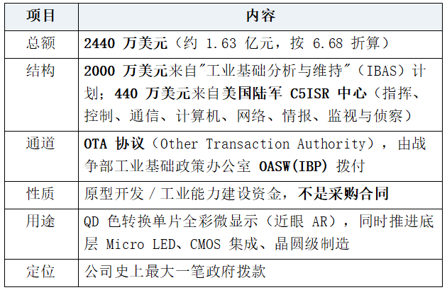
Three benchmarks determine how to interpret this funding.
First, compared with IBAS’s own portfolio.
According to official figures released by the U.S. Department of Defense in 2026, since its inception in 2014, the IBAS program has invested over $5.1 billion across 219 projects, averaging approximately $23.3 million per project. Mojo’s $20 million falls slightly below this average.
This comparison is crucial: it does not represent “the Pentagon heavily betting on a single company,” but rather “incorporating a specific capability into the standard catalog.” IBAS’s KPIs focus on “capability building and production capacity assurance,” not on “how many screens are purchased.”
This funding secures a spot on the production line, not a line item in the order book.
Second, compared with the company’s own fundraising efforts.
The $75 million Series B Prime round completed in September 2025—led by Vanedge Capital, with Marvell as the largest investor, valuing the company at approximately $280 million post-investment—and Crunchbase data showing cumulative funding of around $345 million. The $24.4 million represents about 32.5% of the previous round and 7.1% of total funding—equivalent to 8.7% of non-dilutive capital based on post-investment valuation.
For a company that has burned through $345 million over eleven years without yet achieving mass production, this percentage signifies not a lifeline, but rather “a quarter’s worth of R&D budget.”
Third, compared with the very term “grant.”
OTA is a prototype agreement that follows a streamlined procurement process and carries no purchasing obligations. For the Department of Defense to actually procure goods, it must follow the Program of Record—such as the Army’s Project Management Office system.
Thus, the output of this funding is process capabilities, yield data, and production-line readiness, not revenue.
A detail often overlooked
The press release quotes Assistant Secretary of Defense for Industrial Policy Michael Cadenazzi as stating that “microdisplays are critical to joint forces” and that “ensuring domestic supply of advanced MicroLED displays” is essential. Officially, however, he used the phrase “had previously stressed”—meaning this was a re-packaging of existing policy language, not a new policy stance introduced specifically for this occasion.
The policy weight of this news exceeds its transactional value.
II. Four Paths—Why Color Conversion Specifically?
To understand why this funding went to Mojo, we must first grasp what makes “full-color Micro LED” so challenging.
Micro LED blue-light devices have already reached maturity within the GaN framework, green light is next, while red light remains the most difficult segment: traditional red LEDs rely on AlGaInP, but at micrometer-scale dimensions, sidewall recombination intensifies dramatically, causing efficiency to plummet, and AlGaInP cannot be monolithically integrated with GaN.
Consequently, the industry has divided the challenge of “how to pack three colors onto a single substrate” into four distinct approaches:
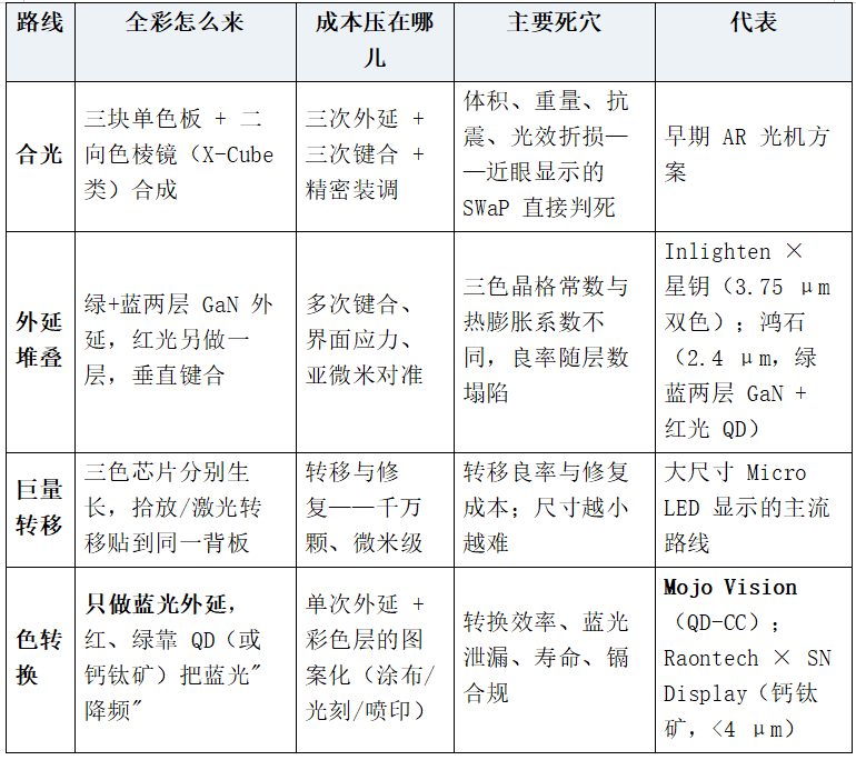
Mojo’s bet is the last option, and it’s a bold one: on an entire 300 mm silicon wafer, only one epitaxial layer (blue light) is grown, while red and green are entirely “converted” via quantum dots. The formation of color layers relies neither on epitaxy nor transfer processes, but instead on post-process coating and lithography.
The industrial logic behind this choice is more noteworthy than its technical rationale.
It shifts the full-color challenge from “III-V epitaxy + massive transfer + packaging” (Asia’s forte) to “silicon-based post-processing + coating and lithography + wafer-level testing” (America’s strength).
Over the past decade, U.S. production capacity in LED epitaxy and packaging has been steadily shrinking:
Cree sold its LED business to SGH in 2021; Nanosys—the leading U.S. quantum-dot materials company—was acquired by Japan’s Shoei Chemical in late 2023–early 2024; eMagin—long regarded as the sole U.S. manufacturer of OLED microdisplays—was bought by Samsung Display in 2023.
By contrast, the U.S. truly excels in 300 mm CMOS production capacity, semiconductor equipment, and materials engineering.
Therefore, when the Pentagon calls for “domestic supply,” a path reliant on Asian epitaxy furnaces and transfer equipment naturally fails to meet the criteria, whereas a route that “grows blue light on a 300 mm silicon wafer, uses lithography for coloration, and ships products after wafer-level testing” can seamlessly close the loop on U.S. soil.
This isn’t a choice based on technological superiority, but rather on what “domestic capacity can deliver.”
Cadenazzi’s original words were “ensure domestic supply of advanced MicroLED displays”—the word “domestic” itself explains why this particular approach was selected.
III. The Physical Tax of Color Conversion
Color conversion sounds like a freebie: one epitaxial layer, three colors. But there are three bills that must be paid.
First: the discount on photon energy, recorded under WPE
When a 450 nm blue photon strikes a quantum dot, it is absorbed and then re-emits a 630 nm red photon. The number of photons may remain unchanged—one enters, one exits—so theoretically, EQE (external quantum efficiency, photon-to-electron ratio) could potentially hold steady.
However, photon energy inevitably suffers a discount: 450/630 = 71.4%. In other words, for every red photon converted, at least 28.6% of the energy turns into heat. Green light (450→530 nm) fares better, with a discount of around 15.1%.

This distinction is important: the energy tax is recorded under WPE (wall-plug efficiency), not EQE. It explains why the color-conversion route appears competitive on “efficiency” metrics, yet inherently lags in “power consumption and heat generation”—precisely the two factors most critical for AR glasses: battery life and thermal management.
This also clarifies why color conversion suits near-eye microdisplays better (smaller area, fewer pixels, controllable absolute power consumption, priority given to brightness), while being ill-suited for large‑size displays (larger area, where 28.6% discounts multiplied across millions of pixels result in tens of watts of wasted heat).
Second: the brightness ceiling, and the significance of the “one million nits” claim
At MicroLED Connect 2026 held in Eindhoven, Netherlands, in September this year, Mojo showcased a single-board RGB display capable of 1 million nits, with both red and green derived from native blue light via quantum dot conversion, and sub-pixel pitch of 1.3 μm, with full-color pixel pitch around 4 μm.
Let’s put these numbers into context: outdoor AR waveguide efficiency typically hovers in the single-digit percentage range, while a panel-level 1 million nits may drop to just 10,000–50,000 nits by the time it reaches the eye. “Ultra-bright” is not merely a descriptive term—it’s a ticket enforced by waveguide efficiency.
What does this mean?
Resolution: a 4 μm full-color pixel pitch corresponds to roughly 6,350 ppi; on a 0.5-inch square silicon wafer, it can accommodate 3K × 3K‑level pixels. For military HUDs, night-vision goggles, or firearm sights, this resolution is far excessive.
Conclusion: Resolution is no longer the bottleneck; brightness and reliability are.
This also explains why the government grant’s mission statement emphasizes “improving brightness and reliability while reducing size, weight, and power consumption,” without mentioning resolution at all.
Third: blue light leakage—civilian use is a color gamut issue, military use is a survival concern
If the QD color-conversion layer isn’t thick enough or doesn’t absorb completely, blue light will leak through. In consumer displays, this manifests as narrowed color gamuts, shifted white points, and reduced contrast—issues of “image quality.”
In night-vision scenarios, however, it’s a different story: a display that appears normal in the visible spectrum might reveal a glowing blue patch in an image intensifier—effectively marking the opponent’s position.
This is an inference drawn from this article (not explicitly stated in official documents): the $4.4 million allocated separately by the Army’s C5ISR Center, rather than bundled into IBAS, likely corresponds precisely to the “operational suitability” requirement—including nighttime signal characteristic management—not merely “getting the screen to work.” IBAS oversees industrial foundations, while C5ISR manages operational needs; the nature of these two funds is fundamentally different.
If this inference holds true, then the “blue light cutoff capability of the QD layer” on this pathway is not an image-quality metric, but a military-regulation standard—its stringency far exceeding any consumer-grade specification.
IV. Eleven Years: From Contact Lenses to a Platform Company
Mojo Vision is no newcomer; its technological foundation predates the “Micro LED hype” by six full years.
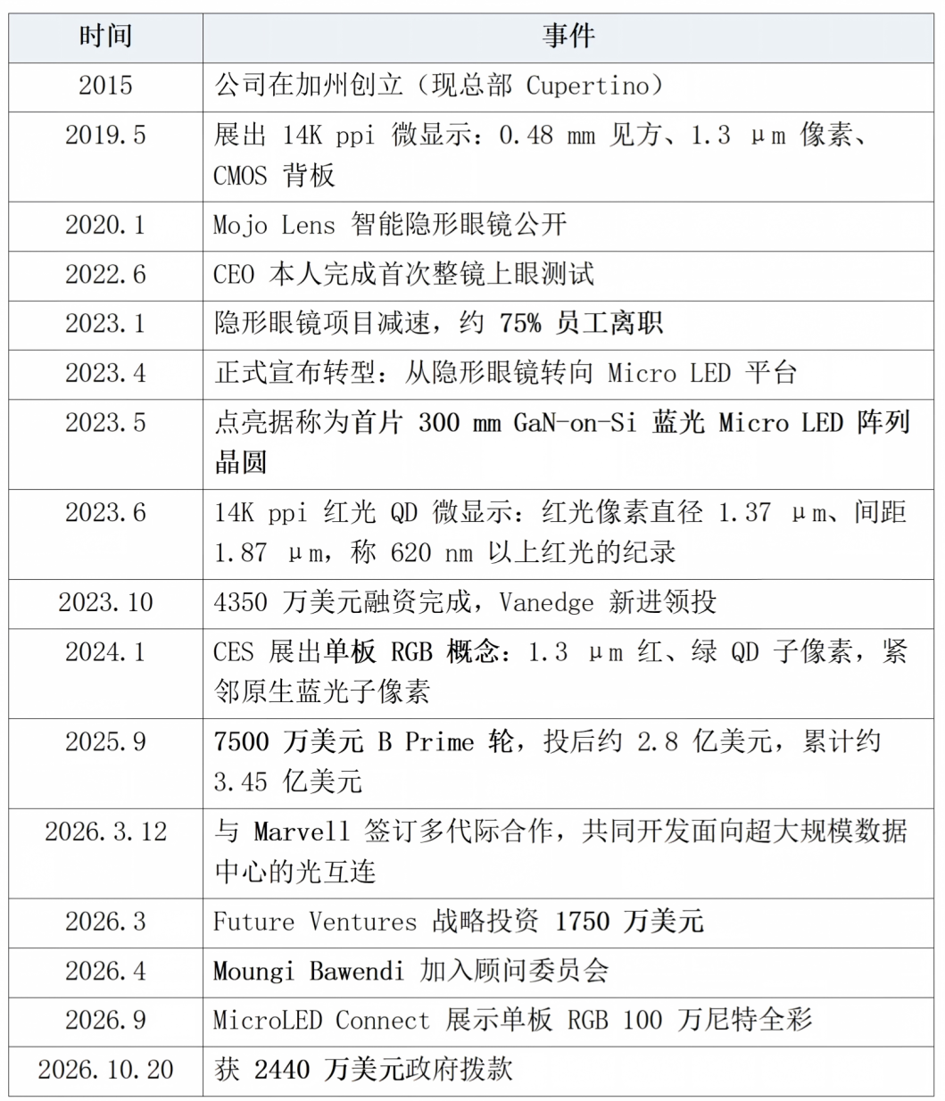
How should we read this timeline? The more than $200 million raised during the contact lens era did not validate whether “lenses can be worn,” but rather whether “1.3 μm pixels can be fabricated on CMOS.” The 2023 transformation wasn’t an admission of failure, but rather a deliberate decision to carve out the most challenging—and reusable—segment—silicon-based microdisplays—for separate sale. The lenses died, but the silicon survived.
From the May 2023 illumination of a 300 mm blue-light wafer, to the January 2024 single-board RGB concept, and finally to the September 2026 million-nit demonstration, the company completed in three years the full journey from “monochrome → dual-color → single-board full-color → high brightness.” Though the pace was slow, each step stood firmly on the same platform—exactly the essence of the term “platform company.”
V. Two Supplementary Backgrounds
1. Bring in Bawendi, not just for name recognition
In April 2026, Moungi Bawendi joined Mojo’s advisory board. He is the Lester Wolfe Professor of Chemistry at MIT and a 2023 Nobel Laureate in Chemistry (shared with Brus and Ekimov), recognized for his discovery and synthesis of quantum dots. His contribution goes beyond simply “discovering quantum dots”; he established a size-controlled, scalable colloidal synthesis method—transforming quantum dots from laboratory flasks into factory-ready materials.
The significance of this appointment must be viewed within a broader context:
- Mojo’s quantum dots are proprietary, not externally sourced;
- Meanwhile, the U.S.’s leading quantum-dot materials company, Nanosys, was acquired by Japan’s Shoei Chemical in late 2023–early 2024, with Shoei’s Japanese production lines commencing operations in March 2024, boasting a capacity equivalent to over 40 million TVs annually;
- Global QD material production capacity and process know-how are largely concentrated in Japan, South Korea, and Germany (Merck).
A company aiming to achieve “material self-sufficiency” on U.S. soil invites the author of “making quantum dots into mass-producible materials” into its fold—this is a standard move toward material sovereignty, not mere PR.
The advisory board also includes former Corning Chief Technology Officer Waguih Ishak (photonics), Anthony Yu, and Rajeeva Lahri. Together, they form a card deck of “materials + photonics + semiconductors,” pointing clearly to the fact that this is not a display company, but a materials-and-process firm.
2. The $75 million Series B Prime and the definition of “platform”
The September 2025 Series B Prime round was led by Vanedge Capital, with Marvell as the largest investor, and included imec.xpand (the venture arm of Europe’s microelectronics research center imec) among new investors. Post-investment valuation stood at approximately $280 million, with cumulative funding reaching $345 million.
Three details worth noting:
- Marvell, as the largest investor, signed a multi-generational cooperation agreement four months later—locking in both capital and technology partnerships simultaneously, indicating that optical interconnects are no “side project.”
- imec.xpand appeared on the list—300 mm GaN-on-Si process maturity largely depends on imec’s 300 mm pilot lines. This capital chain explains why Mojo dared leap from 8 inches to 300 mm.
- The platform checklist comprises seven items: 300 mm silicon architecture, GaN-on-Si micro-lighting devices, efficient optoelectronic detectors, proprietary quantum dots, custom micro-lens arrays, multi-core fiber bundles, and supporting software.
Please note items three and six. Optoelectronic detectors are “receiving-end” components, micro-lens arrays serve to “collect more light into fibers,” and multi-core fiber bundles act as transmission media—only optical interconnects require these three elements; displays don’t need them. Chinese translations commonly omit the “optoelectronic detector” item, yet it is precisely the key to determining the company’s nature.
VI. Dual Platforms: Defense Funds Thin Out Processes for Optical Interconnects
The official press release contains a sentence largely overlooked by Chinese media:
“Advances in underlying Micro LED technology, CMOS integration, and wafer-level manufacturing are expected to strengthen the shared platform between Mojo’s display and optical interconnect businesses.”
Translation: Government funding for improving full-color display yields, CMOS integration, and wafer-level processes will simultaneously benefit AI optical interconnects.
This explains why the company’s capital structure can endure: the display business (AR glasses, defense) serves as the “technological mother body” and gateway to policy resources, while optical interconnects (AI data centers) provide elasticity in valuation. Both share the same production line, the same epitaxy, the same batch of quantum dots, and the same type of micro-lens—the marginal cost is paid only once.
Conversely, Marvell’s commercial partnership provides cash flow expectations and process validation scenarios for the display business. This is the structural advantage of a “dual-platform company” in capital efficiency, and also the reason it has managed to burn through $345 million over eleven years without going bankrupt.
Therefore, this $24.4 million is accounted for as “government funding for the display business,” but strategically, it functions as a subsidy for developing optical interconnect processes. This is the most easily misunderstood aspect of a dual-platform company—you cannot judge solely by which business line it announces.
VII. Cold Water: Five Boundaries Not to Be Overlooked
Boundary One: Grants Do Not Equal Orders.
OTA prototype agreements carry no purchasing obligations, and IBAS outputs are “capabilities,” not “equipment.” Between prototypes and the Program of Record, there are usually three to five years of validation and budget cycles. The direct financial contribution of this funding is to reduce one round of dilution for an unprofitable company.
Boundary Two: “One Million Nits” Has Not Been Third-Party Verified.
This figure comes from the company’s own booth at the September trade show. The Display Tech Center team present on-site issued a public reservation: when QD color conversion claims a single-board exceedance of one million nits, lifespan and white balance must be evaluated concurrently—because brightness, lifespan, and color points on this pathway are mutually constraining variables, raising one often requires sacrificing the other two. This professional reminder deserves citation.
Boundary Three: QD Lifespan Data Remains Unpublished.
The color-conversion layer is subjected to prolonged exposure to high-power blue light, leading to cumulative photooxidation of quantum dots, ligand degradation, and thermal quenching. This is the toughest test facing this pathway, yet currently no publicly available T95/lifespan decay curves exist. Without lifespan data, it’s impossible to declare “mass producibility.”
Boundary Four: Cadmium.
High-performance red QD materials generally contain cadmium (CdSe), relying on RoHS exemptions in the civilian market. Defense procurement, however, is exempt from RoHS constraints—this is both a convenience for this pathway in defense scenarios and a hidden concern: success in defense orders does not guarantee compliance in civilian markets. Consumer-grade AR glasses destined for Europe cannot sidestep this issue.
Boundary Five: Competitors Are Not Absent.
JBD (Shanghai) has completed a $140 million Series B round, Roadrunner platform boasts a 2.5 μm pixel pitch and 10,160 ppi, having achieved mass production of microdisplays and secured design integrations from Xiaomi, TCL, Alibaba, Vuzix, etc.; Hongshi claims to be developing a 2M nits, 2.4 μm pixel pitch solution; Inlighten (U.S.-registered, Starkey contract manufacturer) has exhibited a 3.75 μm green+red dual-color single-board.
Mojo’s differentiation lies in the combination of “monolithic integration + proprietary QD + 300 mm silicon base,” but it is not the only viable solution. Reading this as “the U.S. leads in this round” would be misleading; the accurate narrative is that the U.S. has chosen a path its own production line can support and begun laying infrastructure for it.
VIII. Three Judgments About China
First, this is not “catching up,” but “changing lanes.”
China’s comparative advantages in Micro LED lie in epitaxy, transfer, packaging, and cost curves—this is also why global large-size Micro LED production capacity is concentrated in China. Rather than补课 in areas where it is weak, the U.S. has shifted the question of “how to make color” from epitaxy/transfer processes to silicon-based post-processing. Prediction: By 2027–2028, a narrative of “simultaneous display and optical interconnect production on the same 300 mm platform” will emerge—a form that Chinese manufacturers currently lack.
Second, pinpoint the exact location of the gap.
It’s not about “whether full-color can be made”—China already has layouts for all three color-conversion/stacking pathways; the real gaps lie in three areas:
- Platformization of 300 mm GaN-on-Si (domestic mainstream remains 8 inches);
- Material-process coupling of QD lithography and patterning (this involves triple know-how—formulation + equipment + process window—not something that can be solved simply by buying equipment);
- Reliability verification systems and long-term data collection for military-grade applications.
Third, the optimal strategy may not be chasing 300 mm.
The 28.6% energy tax imposed by color conversion is structural and cannot be eliminated through engineering optimization; epitaxy stacking and massive transfer do not incur this tax, but face yield and cost-related taxes. These two routes will converge head-on on “cost-per-nit” around 2028. Chinese manufacturers’ realistic choice is to push the “epitaxy + transfer + packaging” cost curve below that of the color-conversion route, rather than repeating investments on 300 mm.
Another reminder regarding supply-chain impacts:
Defense orders naturally bring localization requirements and export controls. Procurement of quantum-dot materials, micro-lens arrays, multi-core fiber bundles, and 300 mm epitaxy equipment will become further regionalized.
Domestic manufacturers producing QD materials and micro-optics will simultaneously face pressure from “civilian customers seeking cost reductions” and “overseas customers demanding non-Chinese supply chains”—this isn’t bad news, but requires preemptive side‑choosing.
IX. What to Watch Next
1. Is There a Program of Record?
If, within 12–24 months, C5ISR adds supplementary funding or the Army’s Project Management Office initiates a formal project, it indicates that this pathway has moved from “capability building” to “equipment procurement.” This is the most important single signal.
2. Third-Party Verification of Brightness and Lifespan.
Whoever first presents both “one million nits + T95” figures simultaneously (ideally measured by a complete device manufacturer or a military lab) will truly cross the threshold.
3. Yield and Wavelength Uniformity on 300 mm.
Quantum-dot conversion is sensitive to the wavelength of the blue-light pump; overall wavelength uniformity directly determines color-point consistency—this is a unique engineering challenge exclusive to the 300 mm pathway, and the key to realizing its relative advantages over 8 inches.
4. Nodes of Marvell’s Optical Interconnects.
The 2027 prototype/order rhythm will determine whether the company’s valuation narrative leans toward “display” or “interconnect.”
5. Domestic Trends in 12-Inch Silicon-Based GaN.
If domestic 300 mm GaN-on-Si pilot lines emerge (whether for power or display purposes), the “lane-changing” event will transform into a “lane-sharing” scenario.
Final Thoughts
While $24.4 million is a small figure in the semiconductor industry—too small to buy even a high-end lithography machine—it has secured three key outcomes: placement on the U.S. defense industrial base’s capability list, a rationale linking “materials–process–production line,” and time for the company to continue turning its sunk $345 million into assets.
The real highlight lies not in the amount, but in the U.S. choosing to leverage its existing production capacity to define the next-generation full-color Micro LED process pathway. Competition over technological routes has never been merely about efficiency numbers; it’s always about “which pathway can close the loop within its own supply chain.”
This principle applies equally to China—though the answers differ.
China Light
The official website of the China Association of Lighting Industry and a full-media platform for the lighting sector. We provide authoritative and timely lighting information while striving to be a growth partner for businesses. From brand promotion and channel expansion to consulting, talent training and participation in standards development, we provide comprehensive professional services to help businesses improve quality and efficiency and jointly advance the high-quality development of the lighting industry.
Business Contacts
仇纯 (Ms.): 158 6155 3579
顾君 (Mr.): 137 7157 5253