
Japan successfully developed a mid-wavelength ultraviolet semiconductor laser, expanding new possibilities in optical science.
Introduction
Small, high-efficiency, low-power semiconductor lasers are a type of light source with controllable wavelength and phase. Infrared, red, green, and blue lasers have been commercialized; in recent years, the industry has demanded higher-energy ultraviolet lasers. Professor Motoaki Iwatani of the Graduate School of Science and Engineering at Meijo University, utilizing independently developed semiconductor technology and new methods, invented the world's first "mid-wavelength ultraviolet semiconductor laser". This achievement opens new possibilities for optical science and is not only applicable to industry but also holds promise for addressing challenges in chemistry, environmental science, medicine, and biological sciences.
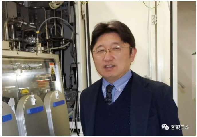
Motoaki Iwatani
Professor, Faculty of Science and Engineering, Meijo University; elected CREST Research Representative in 2016
Research starting in the 1950s
challenges unexplored areas
With fixed wavelength and phase, 'laser' exhibits excellent directivity and convergence, and is widely used in optical discs, laser printers, optical communications, etc., becoming an indispensable part of daily life. In particular, semiconductor lasers, compared with gas lasers and solid-state lasers, possess superior properties such as small size, high efficiency, long lifespan, and high productivity, leading to their widespread application.
Semiconductor lasers adopt a structure (Fig. 1) where an 'active layer' is sandwiched between an n-type semiconductor, in which free electrons carrying negative charge are the majority carriers, and a p-type semiconductor, in which free holes carrying positive charge are the majority carriers. By adopting this structure, the function of an optical resonator that confines light to form standing waves is also achieved. After applying voltage, free electrons in the high-energy n-type semiconductor and free holes in the p-type semiconductor are injected into the active layer and recombine.
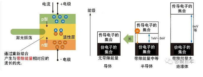
Figure 1: Mechanism of semiconductor lasers (left) and energy states of electrons (right)
The energy generated by recombination, i.e., the bandgap energy of the material, undergoes photoelectric conversion to produce laser oscillation. The bandgap is an energy range where no electronic states exist, determined by the semiconductor material. The larger the bandgap, the greater the energy of the light oscillation.
After this theory was proposed in the 1950s, comprehensive development began in the 1960s. It started with the infrared region, which has lower energy and longer wavelengths, and gradually expanded to regions with higher energy and shorter wavelengths such as red → green → blue (Figure 2). Subsequently, there was growing expectation to achieve semiconductor lasers in the ultraviolet region with even higher energy. However, achieving this goal requires producing high-quality semiconductor materials with a large bandgap of over 3 electron volts (eV) and injecting large currents that generate optical gain to excite the laser into oscillation.
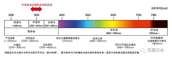
Figure 2: Types of light and the region not yet achieved by semiconductor lasers
To this end, researchers worldwide have competed to develop long-wavelength ultraviolet semiconductor lasers in the 320–380 nm (nm = one billionth of a meter) range, which were developed in 2003, and short-wavelength ultraviolet lasers below 280 nm in 2019. The last unachieved region is the UV-B semiconductor laser in the medium-wavelength range of 280–320 nm, widely known as the cause of sunburn. Tackling this challenge is the project "Realization of Deep Ultraviolet Semiconductor Lasers and Research on Ultra-High Concentration Impurities/Polarized Semiconductors," led under the CREST program "Next-Generation Optical Fundamental Technologies Based on New Light Functions and Properties," with Professor Motoaki Iwanaga of Nagoya University's Faculty of Science and Engineering as the principal investigator.
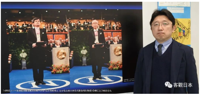
Iwanaga is one of the students of Dr. Isamu Akasaki (who passed away in 2021), who received the 2014 Nobel Prize in Physics for "inventing high-efficiency blue LEDs that enable bright, low-power white light sources." Iwanaga has been under Dr. Akasaki's guidance for over 20 years since his undergraduate studies. Iwanaga says that Dr. Akasaki taught him many things, including his views on technology and research, mental preparation as a researcher, thinking methods and approaches, and analytical perspectives. "He read all my papers and provided accurate comments and suggestions line by line. Without exaggeration, if I had not met Dr. Akasaki, I would not have embarked on a research career" (Iwanaga).
In the field of electronic material physics, it was originally believed that mid-wavelength ultraviolet semiconductor lasers could not be developed. This is because semiconductor lasers require semiconductor materials with a bandgap energy of 3.8–4.4 eV, but materials with a bandgap energy greater than 3 eV exhibit high insulation properties. In other words, it would be necessary to pass a large current essential for laser oscillation through an insulating material—a seemingly impossible dilemma. Additionally, to manufacture stable semiconductor lasers, new materials with few crystal defects and high quality must be developed.
Based on this common sense that such a goal was unachievable, most researchers did not conduct research on mid-wavelength ultraviolet semiconductor lasers. However, Iwata believed, "If we are going to do it, we should challenge a problem that others cannot solve," and thus courageously decided to take on the challenge. Although he tried developing various materials using different methods, each attempt ended in failure, and his resolve gradually wavered.
After several years of research, Iwata decided to give up and shared this idea with Dr. Akasaki. Iwata recalled that upon hearing this news, Dr. Akasaki, who was usually gentle, suddenly became furious. He said, "Is your determination only this much? You have involved so many students; can you bear the responsibility? If you give up for this reason, you might as well stop doing research altogether." From that day on, Iwata renewed his challenge.
Achieve the world's highest quality AlN
by fabricating the AlGaN layer through three-dimensional growth
Iwatani thus expanded its research触角 to various fields, proposed all possible hypotheses, and attempted various methods and materials for development. Hundreds of prototype samples were produced. After repeated trial and error, it finally began to feel like progress was being made around 2014, four years after restarting the research. Starting from when CREST adopted some ideas in 2016, certain concepts gradually took shape. Specifically, these are: 'high-temperature heat treatment of aluminum nitride (AlN) formed by sputtering', 'fabrication of high-quality aluminum gallium nitride (AlGaN) via three-dimensional growth', and 'polarization doping' (Figure 3).
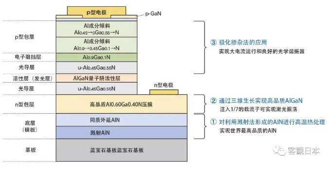
Figure 3: Cross-sectional view of semiconductor laser and three breakthrough technologies used in each layer
For n-type cladding to generate high-quality AlGaN crystals, two-dimensional crystal growth was initially used. However, during the growth process, numerous crystal cracks and lattice defects known as dislocations form, making it impossible to obtain high-quality crystals capable of sustaining laser oscillation. Generally, the presence of cracks and dislocations reduces luminous efficacy; therefore, the threshold for optically pumped lasers did not reach the expected value of 210 kW/cm².
Previously, the substrate and the crystal grown on it required matching lattice constants such as axis length and angle. A lattice mismatch exceeding 1% made it impossible to obtain high-quality crystals. When developing blue LEDs, Dr. Akasaki also faced the same challenge; to solve this, he developed low-temperature deposition buffer layer technology. This is a method of growing gallium nitride (GaN) crystals after depositing aluminum nitride (AlN) on a sapphire substrate. This yielded flat GaN crystals with few defects, leading to the successful invention of blue LEDs.
Although three-dimensional growth methods are rarely used in research on AlGaN-based materials, Iwaki followed Dr. Akasaki's approach for crystal fabrication. Iwaki utilized high-quality AlN generation technology developed by Professor Hidehito Miyake of the Graduate School of Regional Innovation Studies at Mie University, which has gained widespread application in recent years as an AlN template fabrication method for UV LEDs. Using a sputtering method where nitrogen plasma collides with AlN as a raw material and the ejected molecules adhere to the substrate, AlN films were stacked onto a sapphire substrate. The fabricated crystals accumulated in a microcrystalline state, but through heat treatment at 1700°C, highly crystalline AlN films with very few crystal defects were successfully obtained (Fig. 4).
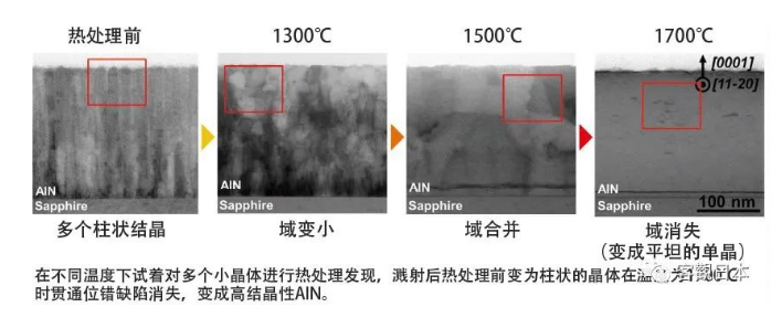
Figure 4: Changes in AlN after high-temperature heat treatment
Iwatani used this AlN as a template and grew AlGaN three-dimensionally on it (Figure 5). There is also a large lattice mismatch of over 1% between AlN and AlGaN, so the process was not smooth, and various conditions were tried. Iwatani smiled and said: 'Development took about 3 years, but thanks to the students' efforts, the threshold power density of the optically pumped laser was reduced to about one-seventh of that during two-dimensional growth, i.e., 36 kW/cm².' A method to reduce it by half further has now been established.
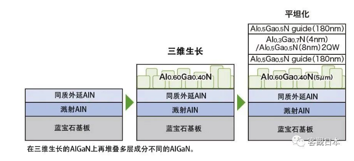
Figure 5: Process for producing high-quality AlGaN using the three-dimensional growth method
即使是辛苦完成的晶体,不能产生激光振荡也没有任何用处,但向具有大带隙能量的晶体注入大电流并非易事。另外,半导体激光器为控制光,需要膜厚大于光的波长,而常规半导体工学中常用的通过添加杂质来控制传导性的方法无法实现激光振荡所需的大电流密度运行。因此岩谷将目光转向了极化掺杂。
一般来说,半导体晶体是电中性的,但氮化物半导体由于对称性低,具有较大的极化电荷。极化掺杂是利用这种极化电荷来产生导电载流子的方法(图6)。极化是绝缘体材料使用的概念,但利用这种极化效应可以产生自由电子和自由空穴,美国圣母大学的研究团队宣布利用极化成功改善了蓝色LED的特性。
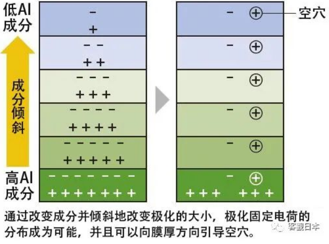
Figure 6: Composition gradient of p-type cladding
This study applied polarization doping to p-type cladding layers, altering the composition of AlGaN material to gradually change the magnitude of polarization (Fig. 7). This enabled the distribution of polarization-induced fixed charges. In 2019, current injection for laser oscillation and the formation of an optical resonator were simultaneously achieved. Using a novel approach not found in conventional semiconductor engineering, we overcame the previously considered impossible challenge of "making non-conductive materials conductive."
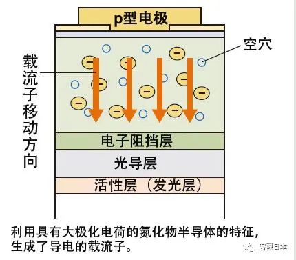
Fig. 7: Polarization doping (Al composition gradient)
Evaluation at room temperature of prototype devices fabricated using these three methods confirmed that they can achieve the light emission modes and spectrum characteristic of semiconductor lasers (Figs. 8, 9). Therefore, Iwatani announced in February 2020 the invention of the world's first mid-wavelength ultraviolet semiconductor laser. He recalled that before the paper was published, he repeatedly answered questions from peer reviewers. "Since it was a global first, naturally there were inquiries about whether it was truly achieved. I submitted many proof documents, and when it finally passed review, I was naturally very happy."
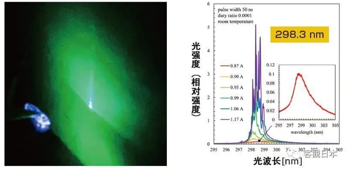
Figure 8: UV-B laser oscillation (left) and the emission spectrum of the UV-B laser during oscillation (right)
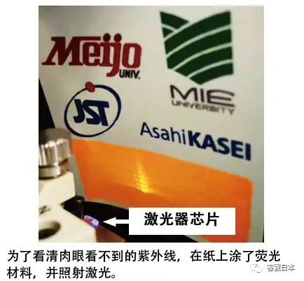
Figure 9: UV-B laser oscillation
This invention caused a sensation immediately upon its announcement both domestically and internationally. The development of innovative semiconductor components was highly praised as an achievement of great importance not only to crystal growth science but also to the advancement of semiconductor engineering, with academic societies and major media outlets reporting on it extensively. It can be said to have illuminated the future of optical science and semiconductor engineering.
The semiconductor laser developed in this project has a wide range of applications and a significant impact. Compared with gas lasers and solid-state lasers operating in the same wavelength range, it enables substantial miniaturization, lower power consumption, longer lifespan, and reduced cost. Common gas lasers measure 1 to 2 meters in size, whereas semiconductor lasers are approximately 1 centimeter—less than one percent of that size. Power consumption is also about one percent of that of gas lasers, and the lifespan reaches roughly 100 times longer, extending from 100 hours to 10,000 hours.
If mass production is achieved, prices will also drop, potentially falling below one hundred-thousandth of those of gas lasers. Iwata emphasized: "History has shown that a new discovery can change the world overnight. If devices using this laser become widespread, they should enable exploration of worlds previously unseen." In the fields of medicine and bioscience, it is highly likely to realize DNA sequencers for analyzing DNA base sequences and other research and medical applications that were impossible with lasers of other wavelength ranges.
Furthermore, by changing the crystal composition, it is expected to generate lasers across all wavelengths in the medium-wavelength range; joint research with universities and companies both domestically and internationally has already begun. Iwata is at the forefront of this research, focusing on the next era and actively engaged in further technological innovation studies. He always keeps in mind a motto stated by the late Dr. Akasaki: 'Results that can rewrite textbooks are super-first-class research.'
Original: JSTnews May Issue
Translation Editor Source: JST Objective Japan Editorial Office